| VIAS Encyclopedia provides a collection of tables and definitions commonly needed in science and engineering. |

|

Home  Electronics Electronics  Diodes Diodes  Schottky Diode Schottky Diode |
||||||||||||||||||||||||||||||||||||||||||||||||
| See also: Walter Schottky | ||||||||||||||||||||||||||||||||||||||||||||||||


|
||||||||||||||||||||||||||||||||||||||||||||||||
Schottky Diode
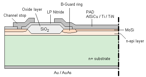
The following illustration shows the structure of a Schottky diode. The metal semiconductor contact made of molybdenum/silicon represents the barrier. In the junction region between insulator, metal and semiconductor, a degradation of the barrier arises as a result of an abrupt change in the surface states. There, substantially higher reverse and forward currents would flow, which could impair the reliability of the diode. A complementarily doped guard ring on the semiconductor fixes this, concentrating the current through the diode on the actual diode region by increasing the barrier.
At the outside edge, a channel stop with an attached n-region and a connection to the back serves to further isolate the channel. From the numerous Schottky diodes available, the following table lists some of the most important examples. Apart from the maximum voltage and current values, the overall capacitance CT (total) at 1 MHz and the forward bias voltage VF at 1 mA indicated.
|
||||||||||||||||||||||||||||||||||||||||||||||||
Home  Electronics Electronics  Diodes Diodes  Schottky Diode Schottky Diode |
||||||||||||||||||||||||||||||||||||||||||||||||
Last Update: 2005-04-07


