| Transistor Basics is a free introductory textbook on transistors and their basic applications. See the editorial for more information.... |

|
Home  Transistor Amplifiers Cascade Operation Overall Power Gain Transistor Amplifiers Cascade Operation Overall Power Gain |
||||


|
  |
|||
|
Design Considerations - Overall Power GainAuthor: Leonard Krugman In any given problem requiring more than one stage of amplification, several cascade arrangements are possible. This flexibility is a desirable design feature; however, it complicates the problem of selecting the best combination of the three general forms of transistor connections with respect to the input and output resistances, and to the required gain of the system Every design is fixed to some extent by the function of the circuit, but the requirement for maximum gain is invariably included.
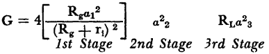
Fig. 5-16. Block schematic of cascade operation Figure 5-16 is the block schematic of a three stage circuit. It is evident from inspection that the overall current gain of the system is the product of the individual stage gains, thus α = α1α2α3. The operating gain as defined in equation 3-45 is
which can be modified to
Since the current gain as defined in equation 3-8 is:
This is a useful form of the equation. For the cascade stages, illustrated in Fig. 5-16, the overall power gain based on equation 5-1 can now be written as
On this basis, a cascade system has maximum gain when each of the stages is separately designed for a maximum value of its associated gain factors. Selection of Stage Connection. The first stage requires that its gain factor
It must be noted that the intermediate stage represented by the current gain α2 in this discussion may actually consist of several intermediate stages having a total current gain equal to α2. This analysis of the three-stage circuit of Fig. 5-14, therefore, is applicable to any number of cascaded stages. In the final stage, the gain factor RLα32 is made as large as possible. The following general rules for this stage are based on the analysis of the gain factor vs RL characteristic for the three basic transistor connections.
(The numerical values listed above apply to those junction transistors with characteristics similar to the Western Electric Type 1752 transistor; however, the general values can be extended on a relative basis to cover all types.) Based on the foregoing rules, it might appear that the choice of the grounded emitter connection is the best under all conditions. However, specific design problems often dictate the use of grounded base and grounded collector circuits when the coupling network, biases, feedback, and other factors are taken into consideration.
|
||||
| Home Transistor Amplifiers Cascade Operation Overall Power Gain |
|
|||


 , and the input resistance as defined by equation 3-13 is ri = r11 -
 , these values may be substituted in the operating gain equation, which then becomes
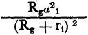 be as large as possible. The following general rules for this stage are based on an analysis of the gain factor vs Rg characteristic:
Last Update: 2010-11-17